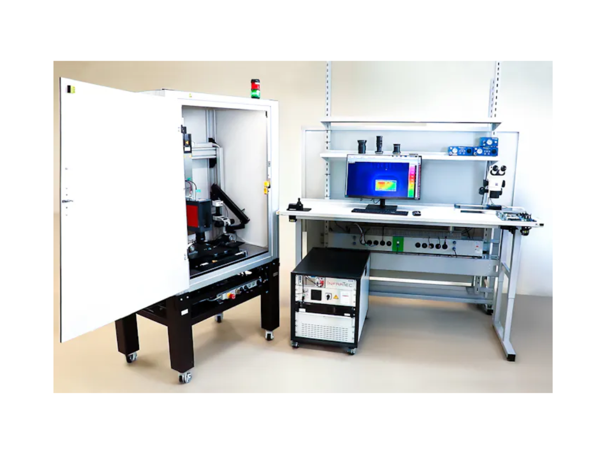
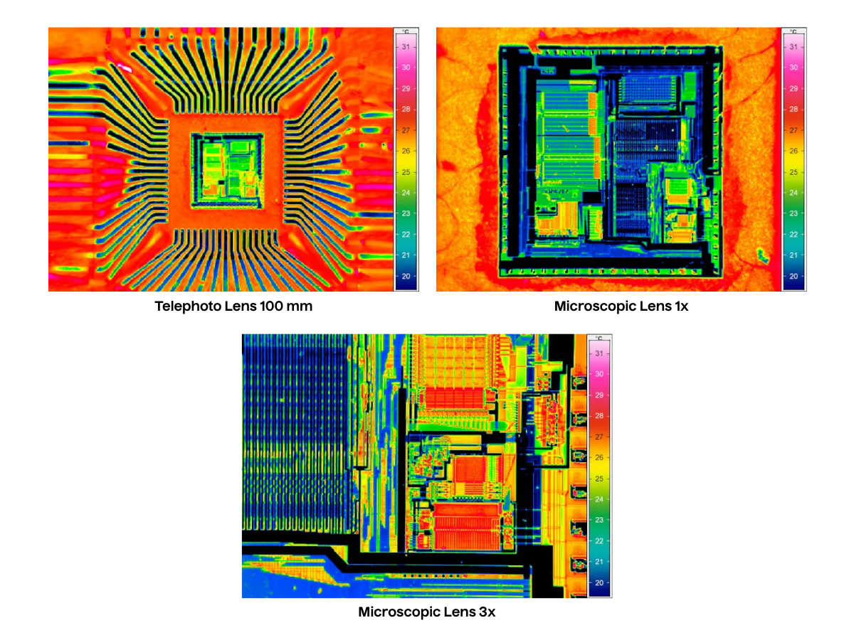
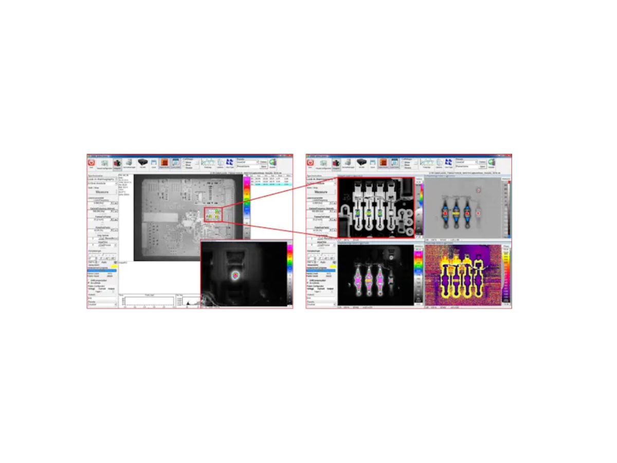
E-LIT delivers complete failure analysis capabilities across multiple levels of electronic assemblies. From entire circuit boards to microscopic semiconductor structures, the platform provides detailed thermal and geometric analysis within a single workstation. High-resolution infrared cameras and microscope optics enable geometric resolutions as fine as 1.3 μm per pixel.
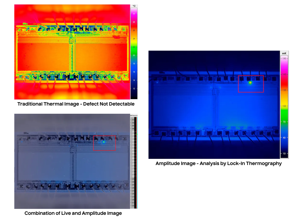
Semiconductor Failure Analysis: Rapidly identify and localize defects within integrated circuits, semiconductor dies, power devices, and packaged components. E-LIT supports both development and production environments where fast and accurate fault isolation is critical.
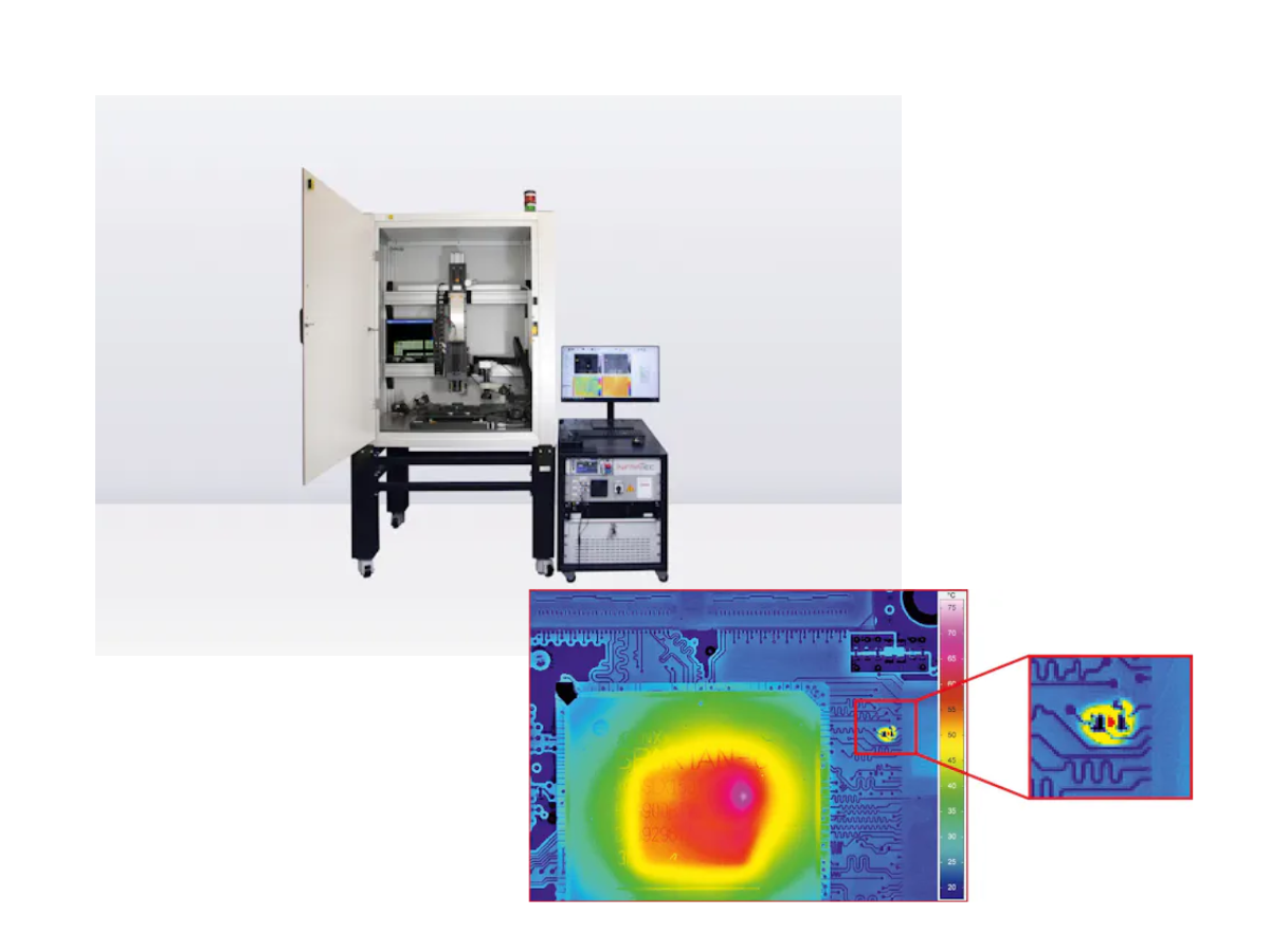
PCB and Electronics Inspection: Detect manufacturing defects and reliability issues in printed circuit boards, including shorts, soldering defects, overheating components, and electrical connection failures.
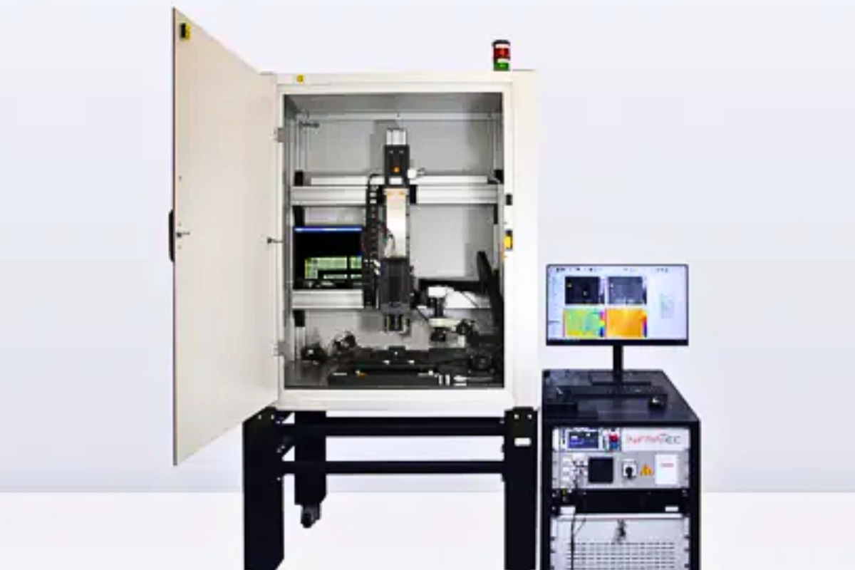
Quality Assurance and Process Control: Integrate lock-in thermography into quality control processes to identify defects early, improve production yields, and reduce costly downstream failures. E-LIT provides a non-contact inspection method suitable for both laboratory and production environments.
Advanced Packaging Validation: Analyze thermal behavior and defect locations in advanced semiconductor packaging technologies, including stacked-die devices, multi-chip modules, and complex electronic assemblies.